Home
>>
Technical Platform
>>
Detection Platform
>>
TEM & SEM Services
Download Center
Quick Inquiry & Consultation
TEM & SEM ServicesIntroduction

Scanning Electron Microscopy (SEM) uses a high-energy electron beam to scan the surface of a sample. The interaction between the electron beam and the sample generates signals such as secondary electrons, backscattered electrons, and X-rays. These signals are collected by detectors and converted into images, revealing the surface morphology of the sample.

Transmission Electron Microscopy (TEM) is a technique in which a high-energy electron beam is transmitted through an electron-transparent sample (~100 nm thick). The interaction of electrons with the sample produces scattered and transmitted electrons, forming high-resolution two-dimensional images. Unlike SEM, Scanning Transmission Electron Microscopy (STEM) focuses the electron beam into a narrow point and scans the sample in a raster pattern. By using TEM or STEM, high-quality images with atomic-level resolution can be obtained. These images are widely used in cancer research, virology, materials science, and other fundamental studies.

KMD Bioscience offers comprehensive SEM and TEM services covering the entire workflow, from sample production to image analysis. Our professional team has extensive experience and advanced technical expertise to ensure the accuracy and reliability of results. We provide customized solutions tailored to meet diverse customer requirements. SEM enables observation of micro-surface morphology, such as cellular structures and surface defects, while TEM provides detailed insights into internal structures, such as lattice arrangements and nanoparticles.
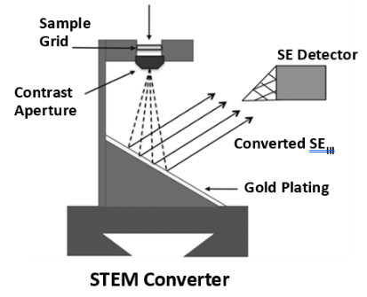
扫描透射电镜-卡梅德科技.png

TEM and STEM offer superior spatial resolution compared to SEM. However, compared to conventional analytical tools, these methods require more complex sample production and longer processing time. To obtain high-resolution structural and functional information, all samples should be preserved in their original state with a thickness of approximately 100 nm. We provide high-quality and relatively cost-effective routine TEM and STEM sample production services. Our offerings help researchers and their teams achieve specific research objectives.


Comparison between Scanning Electron Microscopy (SEM) and Transmission Electron Microscopy (TEM)

SEM

TEM

Detection Type

Detects secondary electrons or backscattered electrons from the top of the sample.

Detects electrons transmitted through the sample.

Sample Thickness

Samples can be solids, powders, thin films, etc., with no strict requirements on thickness.

Samples must be extremely thin (typically less than 150 nm) to ensure electron beam penetration.

Maximum magnification

Up to 1–2 million times.

Over 50 million times.

Operation

Easy to use, with little or no sample production required.

Not easy to use, requires sample production.

Application

Mainly used for observing surface morphology.

Used for internal structure observation. Sample production is complex and requires ultrathin sectioning.

Service content

Routine fixation, dehydration, and embedding

Specimen sectioning

Negative staining of samples

Specific nanoparticle staining

Nanoparticle size distribution

Immunoelectron microscopy

Phase identification

Electron diffraction

Elemental analysis, virus and particle quantification

Chemical state analysis

In addition to routine services, we can also provide customized services for your special samples and specific requirements.

Delivery content

We collect images of your samples and specimens through TEM and STEM and provide a report that includes:

-- High-resolution images.

-- Elemental analysis presented as point profiles, line profiles, and elemental maps.

-- Professional pathological consultation.

Service advantages

-- Our Scientists provide both standard and customized services to meet specific customer requirements.

-- We offer a one-stop service: from project design to experimental result analysis, saving time for customers.

-- We utilize advanced technologies to shorten experimental timelines.

-- We provide high-quality services and competitive pricing for clients.

Frequently Asked Questions

1. Why use Transmission Electron Microscopy (TEM)?

Answer: TEM can address many questions about high-resolution structures, including diseased tissues, bacterial and viral structures, cultured cells, and artificial materials such as support films and particle suspensions.


2. Why must the samples be so small?

Answer: The chemicals used for fixing tissues to achieve high resolution penetrate at a slow rate.


3. What advantages does TEM have over optical and/or fluorescence microscopy?

Answer: The primary advantage of TEM is its higher resolution compared to microscopes that use visible light.


4. Can any material be used for TEM?

Answer: TEM has strict requirements for samples, mainly regarding thickness, conductivity, stability, and structural properties. For example, TEM requires sample thickness between 50–100 nm to ensure electron beam penetration; TEM samples must possess certain conductivity to prevent charge accumulation; samples must remain stable under high-energy electron beams; TEM is suitable for observing crystalline materials, especially crystal defects and interfaces. For specific sample inquiries, please consult our sales support team.

Login

Don’t have an account?Sign Up Now

Register

Already have an account?Log In Now